
Automatic Gate Light Circuit Best Engineering Projects
This schematic diagram shows the arrangement of four OR gates within a standard 4071 CMOS integrated circuit. OR gates are basic logic gates, and are available in TTL and CMOS ICs logic families. The standard 4000 series CMOS IC is the 4071, which includes four independent two-input OR gates. The TTL device is the 7432.
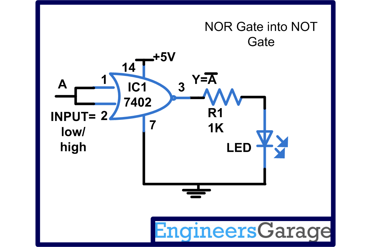
circuit diagram of nor gate
A logic circuit diagram for a 4-bit carry lookahead binary adder design using only the AND, OR, and XOR logic gates. CMOS diagram of a NOT gate, also known as an inverter. MOSFETs are the most common way to make logic gates.
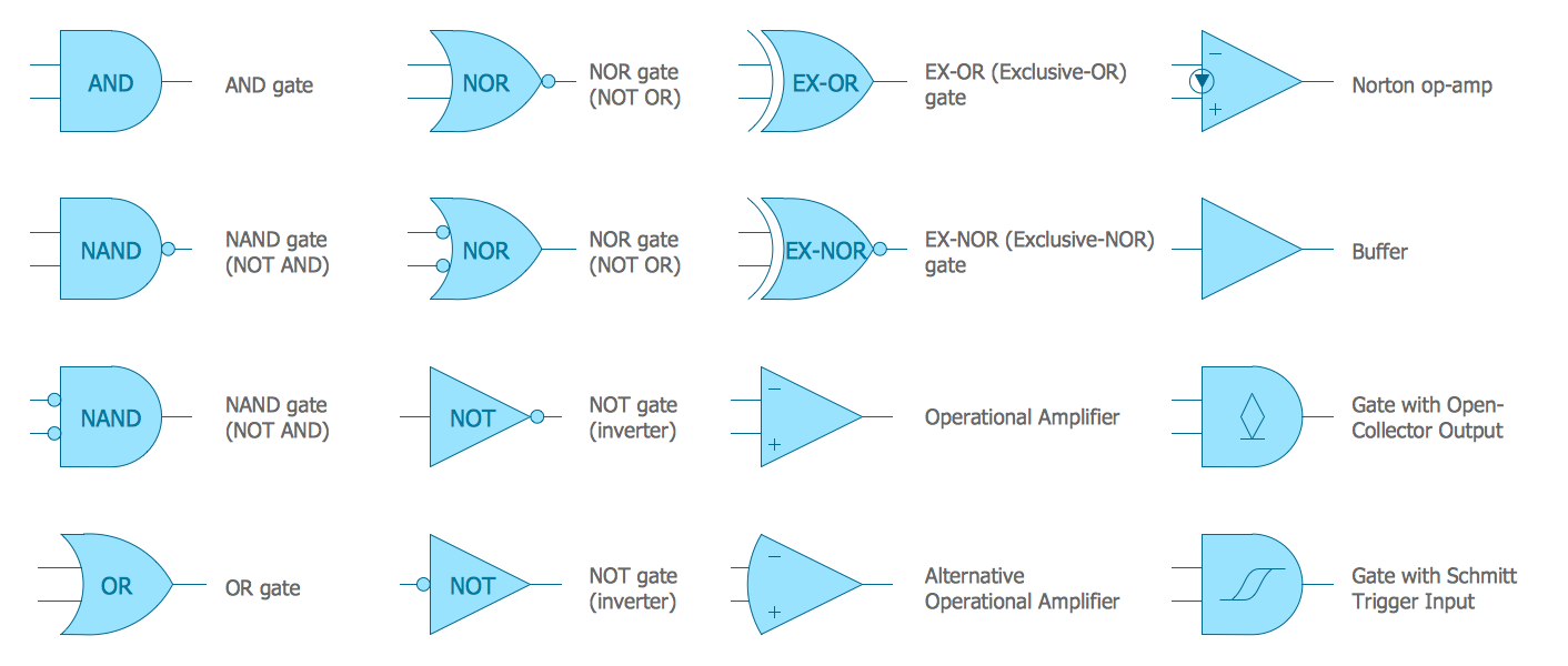
Electrical Symbols Logic Gate Diagram
1 + 1 = 1 The symbol of the OR type logic gate is shown below: Basic OR Gate Here, X and Y are considered as inputs and Z is the output. The X and Y inputs can be either '0' or '1'. It may have multiple inputs but has only one output. With this, the logical formula is given as X + Y = Z
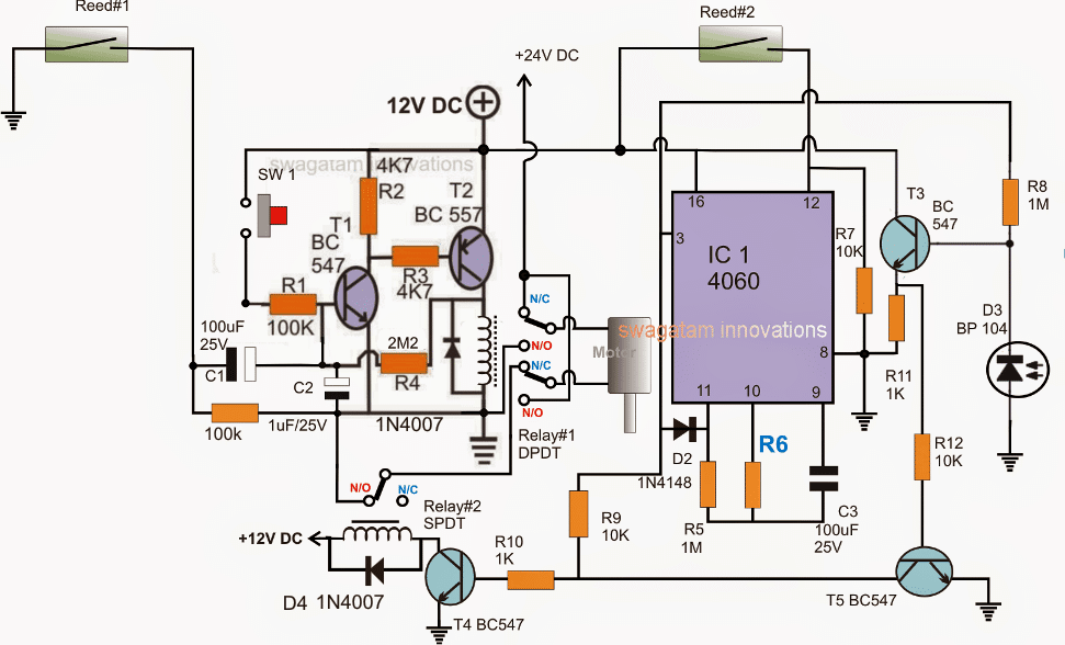
Automatic Sliding Gate Controller Circuit Homemade Circuit Projects
The OR Gate Schematic Diagram is comprised of two main parts: the inputs and the output. Inputs are the signals that come into the circuit, while the output is the result. This output is either a 0 (false) or 1 (true) depending on the logic of the circuit.

schematic diagram of or gate Circuit Diagram
The logic gate level circuit diagram of the OR gate built using NOR gates is shown above. This is a simple diagram that shows where the input and output connections should be made. The component level circuit diagram for OR gate 4 is shown above. This calls out that 2K resistors should be used as well as a 5-volt power supply.
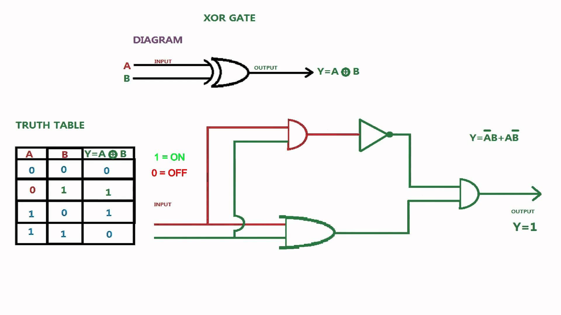
[DIAGRAM] Block Diagram Xor
The Logic OR Gate is a type of digital logic circuit whose output goes HIGH to a logic level 1 only when one or more of its inputs are HIGH The output, Q of a "Logic OR Gate" only returns "LOW" again when ALL of its inputs are at a logic level "0". In other words for a logic OR gate, any "HIGH" input will give a "HIGH", logic level "1" output.

Digital Logic Gate Full Cheat Sheet
(Working Principle & Circuit Diagram) September 27, 2020 by Electrical4U Contents What is an OR Gate? An OR gate is a logic gate that performs logical OR operation. A logical OR operation has a high output (1) if one or both the inputs to the gate are high (1). If neither input is high, a low output (0) results.
Circuit Diagram Of Xnor Gate Using Nand Gates Only Wiring Diagram
The circuit design of OR gate (by using diodes) is given below. The circuit uses two diodes at input side. In all logic circuits, +5 volts is represented as HIGH level logic and 0 volts or ground is represented as the LOW level logic. The two logic levels are represented as binary numbers 0 and 1.
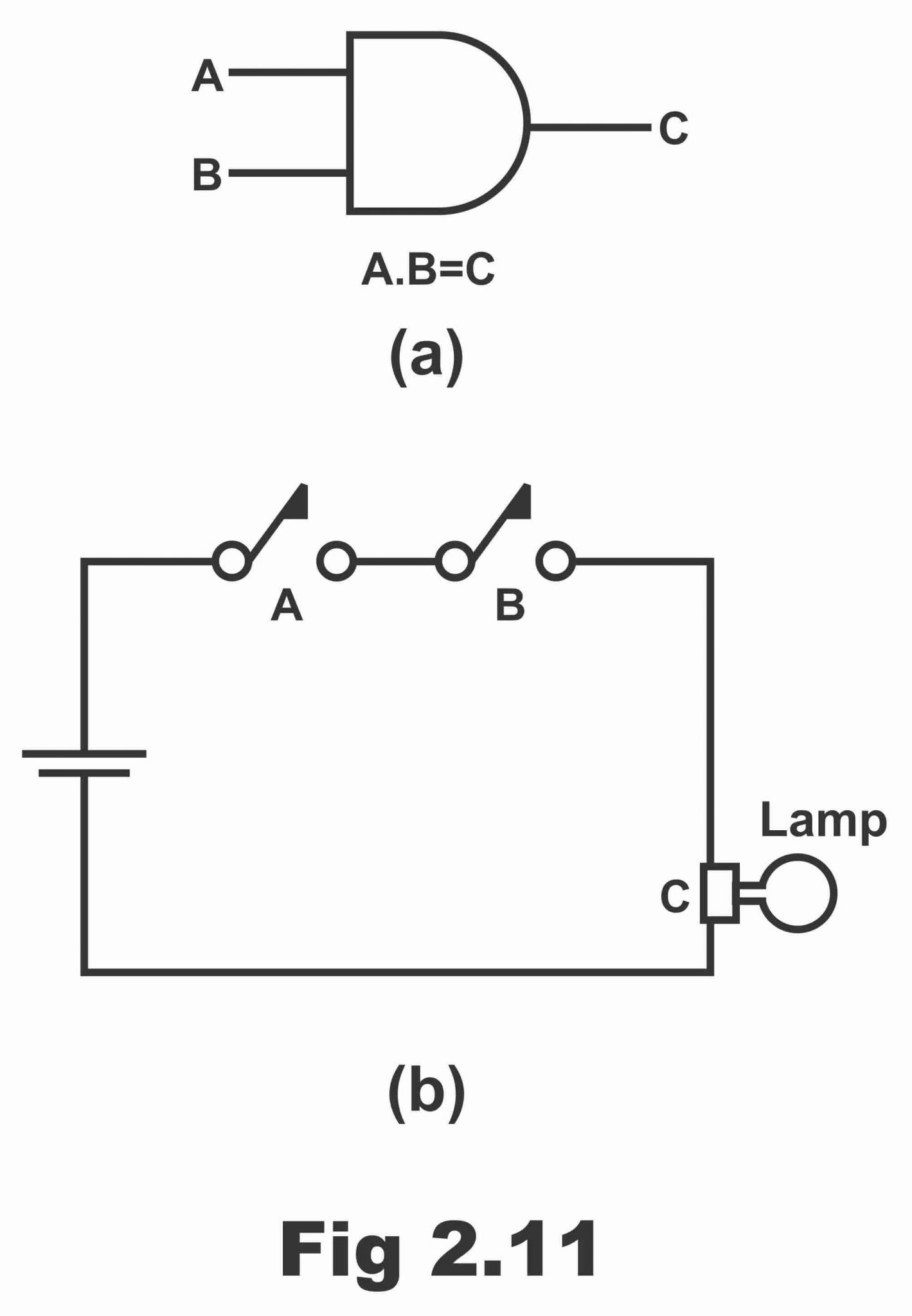
Logic AND Gate Working Principle & Circuit Diagram
OR gate Circuit Diagram. The OR gate can be realised by the electronic circuit by using two ideal p-n junction diodes D1 and D2 as shown in fig. 2. Fig. 2. Here negative terminal of the battery is grounded and corresponds to the logical 0 (low) and positive terminal of the battery (i.e. voltage 5 V in the present case) corresponds to logical 1.
xor gate logic diagram DHNX Wiring Diagram
Logic Gates Circuit Diagram & Working The logic gates are the building blocks of digital circuits. A logic gate has one output, but one or more inputs. The output signal appears only for certain combinations of input signals. There are three basic logic gates: OR gate, AND gate, NOT gate.

Logic Gate Circuit Diagram Headcontrolsystem
OR Gate using Transistor - Circuit Diagram The first version of the OR gate is the simplest one - it consists of two paralleled emitter followers sharing a common emitter resistor. The above circuit diagram shows the simplest way to build an OR gate using NPN transistors.

Smart Gate circuit diagram
OR Gate Circuit diagram using Transistors Let's construct a simple OR gate circuit using transistors to demonstrate the required components and the circuit's functioning. OR Gate using Transistor Components Needed: Resistance, NPN transistor, power supply in voltage, wires, switches Working of the Circuit:

Not Gate Circuit Diagram On Breadboard
Circuit Diagram and Working The truth table of OR gate is show in figure. As in truth table the output of a OR gate should be LOW only if both the gate inputs are LOW. In any other case the output should be HIGH. So if any one or both inputs are HIGH,the output of OR gate will be HIGH.

Free download Logic gate Circuit diagram XOR gate AND gate Electronic symbol, the meridian
We call that a logic circuit. Circuits enables computers to do more complex operations than they could accomplish with just a single gate. The smallest circuit is a chain of 2 logic gates. Consider this circuit: Inputs A and B first go through an AND gate. Then the output of that gate goes through an OR gate, combined with another input, C.

[DIAGRAM] Circuit Diagram Nand Gate
The symbol for an OR gate consists of multiple inputs and a single output, represented by lines entering and exiting the gate, respectively. OR Gate-Symbol, Truth Table, and Circuit Diagram. The primary function of an OR gate is to perform logical OR operations on its inputs. It acts as a combinatorial logic element, allowing the combination of.

GATE AUTOMATION Fence and Deck Depot
OR GATE: Symbol, Truth Table, Circuit Diagram with Detailed Images Last updated on May 17, 2023 Download as PDF Overview Test Series The inputs and outputs of logic gates can occur only in two levels: HIGH and LOW, MARK and SPACE, TRUE and FALSE, ON and OFF, or 1 and 0.